SG2000 Boot Sequence
From Cold Silicon to User Space
2026-09-13
Choosing the Primary Core: ARM or RISC-V
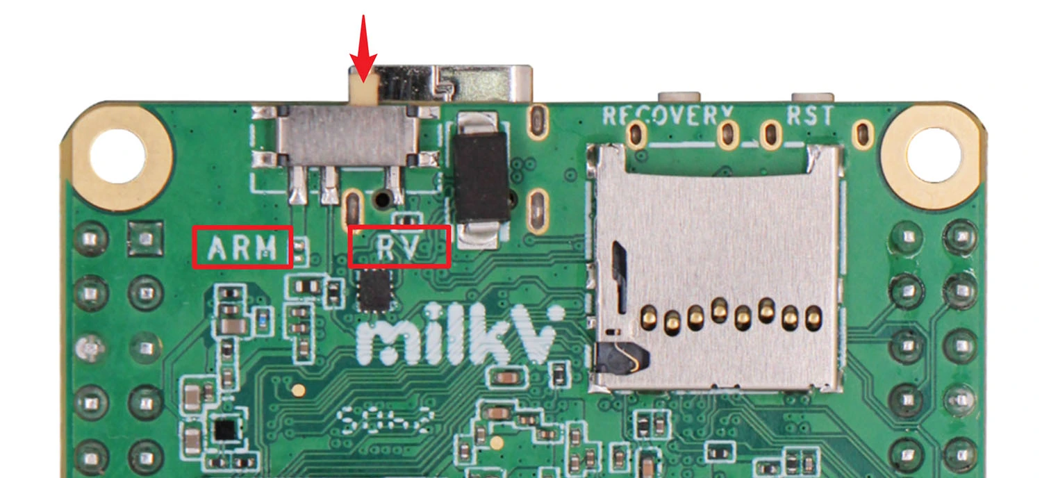
The Duo S carries an SG2000, whose primary core can be either a RISC-V C906 or an ARM Cortex-A53, selected by the boot-mode switch / strap pin shown above (RV vs ARM).
For the rest of this lecture we assume RISC-V mode (RV).
The RV Core Comes Out of Reset
With the switch on RV, the core that comes out of reset is the T-Head C906 main processor. It does not run a loader — it simply starts executing at a hard-coded address:
0x0440_0000
Why there, and why can’t software change it?
- On reset a RISC-V hart enters M-mode with its PC set to an implementation-defined reset vector — there is no code involved.
- On the C906 that vector lives in
MRVBR(CSR0x7C7). The C906 manual says it is “the reset start address transferred to C906 during SoC system integration” and is not writable in M-mode. - The SG2000 ties
MRVBRto0x0440_0000— the base of the on-chip BootROM.
The Physical Memory Map
No MMU is on yet, so 0x0440_0000 is a physical address. The SG2000’s fixed address map places the BootROM exactly there:
| Region | Address range | What it is |
|---|---|---|
| BootROM (ROM) | 0x0440_0000–0x0441_FFFF |
mask ROM — first code to run (BL1) |
| UART0 | 0x0414_0000 |
early serial console |
| RTCSYS | 0x0500_0000 |
POR / reset / RTC |
| RTCSYS_SRAM | 0x0520_0000 |
on-chip SRAM (FSBL/BL2 runs here) |
| PLIC | 0x7000_0000 |
platform interrupt controller |
| CLINT | 0x7400_0000 |
timer + inter-processor interrupts |
| DDR | 0x8000_0000 |
512 MiB DRAM — not usable yet |
The hard-coded boot address lands exactly on the BootROM, so the first fetch is served by mask ROM — the one region guaranteed to work before the PLLs and DRAM controller are brought up.
64-bit Core, 39-bit Virtual, 32-bit Physical
These three widths are independent, and mixing them up is the classic confusion:
| Width | On the SG2000 | Set by | Governs |
|---|---|---|---|
| XLEN | 64 bits | ISA (RV64) | registers, pointer arithmetic |
| Virtual address | 39 bits (Sv39) | MMU mode in satp |
512 GiB virtual space |
| Physical address | 40 bits (core), 32 bits (SoC) | integration | actual bus addresses |
- XLEN = 64 is why pointers are 64 bits — but that says nothing about how wide a physical address is.
- The C906 MMU is Sv39 only: it translates 39-bit virtual addresses to 40-bit physical addresses.
- The SG2000 only decodes a 32-bit physical space (map tops out at
0xFFFF_FFFF), so the upper bits are structurally zero, not discarded.
At boot the MMU is off, so the PC is a physical address:
0x0440_0000 is really 0x0000_0000_0440_0000 — the high bytes just have nothing to say yet.
Inside the BootROM (BL1)
The BootROM is the only code guaranteed to exist and run at power-on: mask ROM at 0x0440_0000 (64 KiB), etched into silicon and immutable.
- Sample the boot straps (
EMMC_DAT0/EMMC_DAT3) → choose the boot device (SPI NOR/NAND, eMMC/SD, or USB/UART download). - Bring up just enough of that device — plus UART — to read it.
- Read the FIP header (
"CVBL01") and load BL2 into on-chip SRAM. - Verify the image if secure boot is enabled (RSA/SHA/AES).
- Publish a ROM API that later stages call.
- Jump to BL2.
Because it can neither be patched nor resized, it does the minimum and hands off. The API survives in the FSBL: p_rom_api_load_image, image_crc, flash_init, get_boot_src, verify_rsa, cryptodma_aes_decrypt.
Selecting the Boot Device
At reset the BootROM samples two strap pins and latches the result in a read-only register, conf_info @ 0x0300_0004:
EMMC_DAT3 |
EMMC_DAT0 |
Device |
|---|---|---|
| ↓ | ↑ | SPI NOR (memory-mapped) |
| ↓ | ↓ | SPI NAND |
| ↑ | ↑ | eMMC |
conf_info.boot_sel[2:0] reads back as 0 = SPI_NAND, 2 = SPI_NOR, 3 = EMMC.
The options divide into two groups (enum boot_src):
- Read from flash: SPI NAND, SPI NOR, eMMC
- Download / recovery: SD, USB, UART (the Duo S has a
RECOVERYbutton)
SD is not a separate strap: SD0 and eMMC share IO (TRM §4.2), so the BootROM reports BOOT_SRC_SD when a card is present — exposed via p_rom_api_get_boot_src().
On the Duo S: hardwired, no jumpers. R51/R52 (10K) fix the (1,1) = eMMC setting; the microSD shares those lines. SPI NOR/NAND need rework.
What Is a Block Device?
There are two very different ways to reach storage on this SoC:
| Memory-mapped | Block device | |
|---|---|---|
| Example | SPI NOR @ 0x1000_0000 |
eMMC, SD, SPI NAND |
| Addressing | any byte address | fixed-size blocks (512 B) |
| Access | plain load / store |
issue a command, read a buffer |
| Random access | direct (XIP) | per-block request |
A block device is addressed in sectors, not bytes. You cannot load a byte from it: you ask the controller for block N, the controller drives the media and deposits the data in a buffer or DMA memory, and only then can you read it.
eMMC and SD are serial devices with a command protocol (eMMC even has a flash translation layer). They live behind a host controller:
- eMMC
0x0430_0000· SD00x0431_0000· SD10x0432_0000 - SPI NAND
0x0406_0000
How SDHCI Works
SD/eMMC controllers implement SDHCI (SD Host Controller Interface), a standard register block the host drives.
| Register | Job |
|---|---|
ARGUMENT, COMMAND |
set the argument, then command index + flags to start it |
RESPONSE0–3 |
the card’s reply (RCA, CID, CSD, …) |
BLOCK_SIZE, BLOCK_COUNT |
how much data to move |
TRANSFER_MODE, SDMA/ADMA |
DMA vs buffer, read vs write, where it lands |
PRESENT_STATE, interrupt status |
ready / busy and completion |
Reading a card is a command sequence: CMD0 → CMD8 → ACMD41 → CMD2/CMD3 → CMD7 → CMD17/CMD18.
For a read, data doesn’t land in a private buffer: you program a physical system-memory address (SDMA_SADDR, or an ADMA descriptor table) and the controller DMAs the block straight into SRAM or DRAM.
The BootROM runs all of this and loads BL2. BL2 never touches the controller — it just calls p_rom_api_load_image(buf, offset, size, retry).
On-chip SRAM Is Not Cache
| L1 cache (C906) | On-chip SRAM | |
|---|---|---|
| Addressing | transparent, tag-based | fixed physical addresses |
| Backing | a copy of DRAM | is the memory |
| Contents | evictable / invalidatable | persist until overwritten |
| Before DRAM | needs a backing region | directly usable as code + data |
| Size here | 32 KiB I / 32 KiB D | 24 + 64 + 100 KiB |
The SG2000 has real dedicated scratchpad SRAM (TCM-like), not “cache-as-RAM” — the C906 has no such mode.
Three blocks the boot chain uses:
RTC_SRAM— 24 KiB @0x0520_0000TPU_SRAM— 64 KiB @0x0C00_0000(shadow0x3C00_0000)VC_SRAM— 100 KiB @0x0BC0_0000(shadow0x3BC0_0000) — BL2 runs here
Life Before DRAM: The SRAM Budget
Until ddr_init() returns, everything runs out of ROM + SRAM:
| Stage | Lives in | Size |
|---|---|---|
| BootROM (BL1) | mask ROM @ 0x0440_0000 |
64 KiB |
| BL2 (FSBL) | VC_SRAM @ 0x3BC0_0000 |
100 KiB |
| DDR params + scratch | sram_union_buf (SRAM) |
a few KiB |
~188 KiB of dedicated SRAM (24 + 64 + 100) versus 512 MiB of DRAM. That asymmetry is exactly why the boot chain is split into many small, progressively larger stages.
Only once DRAM is trained does BL2 load_rest() copy the big payloads — OpenSBI, U-Boot, FreeRTOS — into 0x8000_0000.
Bringing Up DRAM
DDR3 is a separate SiP die behind a controller + PHY. To make it usable:
- Configure the PLLs / clocks (baseline is just XTAL).
- Select the DRAM package (vendor / capacity / type) from
conf_info+ eFuse, then program the controller + PHY with the matching compiled-in sequences. - Run training / calibration (read/write leveling, gate training) using a scratch buffer.
This cannot run from DRAM — DRAM is untrustworthy until after training. The same chicken-and-egg problem, one level down. TRM §15.4.2 notes the init process is “provided in the form of a software package” — black-box code linked into BL2.
The fix happens in BL2: load_ddr() calls ddr_init(), which reads conf_info/eFuse to pick the DRAM config and runs the compiled-in controller/PHY bring-up. After that, 0x8000_0000 is live.
What DRAM Training Actually Does
Training is not a fixed delay table: the PHY measures the board — write patterns, read back, sweep delay/VREF, center each data eye.
| Procedure | FSBL function / register | What it aligns |
|---|---|---|
| Write leveling | cvx16_wdqlvl_sw_req() |
write DQS ↔︎ CK at the DRAM |
| Read valid / gate | cvx16_rdvld_train() |
when to sample read data |
| Per-bit / lane deskew | reg_d*_skew_calib_result |
centers each DQ bit’s eye |
| VREF sweep | phyd_dfi_wdqlvl_vref_* |
optimal input reference voltage |
| ZQ calibration | ZQ Cal Long/Short, GPIO_ZQ |
driver impedance / ODT |
| Pattern stimulus | cvx16_bist_wr_prbs_init() |
known-good data for the sweep |
Why not hard-code the timings?
- DDR3-1866 → one bit ≈ 0.54 ns; alignment is a picosecond problem.
- Fly-by routing + package/PCB skew: CK, DQS, and each DQ arrive at different times.
- The right taps depend on board + DRAM + PVT — unknowable from a datasheet.
The init code and its parameter tables are linked into BL2, not loaded as a blob. Training runs from SRAM (sram_union_buf) — it’s what makes DRAM trustworthy.
BL2’s Last Act: Fill DRAM and Jump
With DRAM live, load_rest() raises the clocks and copies the rest of the FIP into DRAM:
| Payload | From (FIP) | To |
|---|---|---|
| C906L RTOS (optional) | blcp_2nd_loadaddr |
blcp_2nd_runaddr — top of DRAM |
| OpenSBI / ATF (MONITOR) | monitor_loadaddr |
monitor_runaddr = 0x8000_0000 |
| U-Boot (LOADER_2ND) | loader_2nd_loadaddr |
decompressed to runaddr (~0x8020_0000) |
Each image is CRC-checked, signature-verified (if secure boot), and D-cache-flushed. The optional RTOS image then releases the secondary C906L core. Finally BL2 calls jump_to_monitor(...), handing control to OpenSBI and passing the U-Boot entry along.
Resulting DRAM layout: OpenSBI @ 0x8000_0000, U-Boot @ 0x8020_0000, kernel load buffer @ 0x8140_0000, FreeRTOS at the top.
Execution Modes: The Privilege Ladder
RISC-V has three privilege levels. The C906 supports all three and starts in M-mode at reset.
| Mode | Privilege | Can touch | Boot-chain occupant |
|---|---|---|---|
| M-mode | highest | memory, I/O, all CSRs, PMP | BootROM, FSBL, OpenSBI |
| S-mode | middle | S+U CSRs; page tables (satp) |
U-Boot, Linux |
| U-mode | lowest | U CSRs only | applications |
Moving between modes is asymmetric:
- Down — only deliberately, via
mret(M→S/U) orsret(S→U); the target mode comes frommstatus.MPP/sstatus.SPP. - Up — only by trapping: hardware saves the PC to
mepc/sepc, the cause tomcause/scause, and vectors tomtvec/stvec. ecallis a deliberate trap: U→S for a syscall, S→M for an SBI call.
By default every trap goes to M-mode. medeleg/mideleg let M-mode delegate S-level traps straight to S-mode, avoiding a round-trip — exactly what OpenSBI configures before dropping to U-Boot.
Why Two Privileged Modes?
S-mode is not denied physical memory — it’s denied M-mode’s resources.
- S-mode owns virtual memory — it programs
satp(Sv39), builds the page tables, direct-maps RAM, andioremaps MMIO. MMU off (U-Boot) = physical addresses directly. - What it can’t do — M-mode CSRs, M-only instructions, PMP-fenced memory. Platform actions go through an SBI
ecall.
Why split them?
- Portability — one kernel, many SoCs: board quirks hide behind the SBI ABI.
- Security — PMP fences the root of trust from a compromised OS.
- Multiplexing — M-mode can host multiple S-mode domains.
- Classic ladder: ARM EL3/EL1/EL0, x86 ring −1/0/3.
OpenSBI makes the split concrete: medeleg = 0xb109 delegates ecall from U to S-mode (syscalls → Linux) but keeps ecall from S in M-mode (SBI calls → OpenSBI). mideleg = 0x222 sends S-mode interrupts to S-mode.
OpenSBI: The M-mode Runtime
OpenSBI is the reference implementation of the RISC-V SBI (Supervisor Binary Interface) — the M-mode firmware. It’s the FIP’s MONITOR component: fw_dynamic.bin for RISC-V, or ATF bl31.bin in ARM mode.
Why it exists:
- S-mode cannot do platform operations (timer, IPIs, hart start/stop, reset) — those are M-mode-only. SBI standardizes those
ecalls. - It hides board quirks, so one kernel/U-Boot runs on many SoCs.
- PMP lets it fence the root of trust away from the OS.
- It delegates traps so S-mode handles page faults and syscalls directly.
At boot it initializes the hart/platform, sets PMP, programs mideleg = 0x222 / medeleg = 0xb109, then mrets to S-mode U-Boot at 0x8020_0020 with a0 = hart ID and a1 = DTB (0x8008_0000). M-mode stays resident — S-mode still needs its services.
U-Boot: The Bootloader
Das U-Boot (2021.10, cvitek_cv181x) is the S-mode bootloader. Its job is flexible OS loading — filesystems, network, scripts, interactive console.
What it does:
- Initializes storage and I/O: MMC/SD, Ethernet, USB, serial console.
- Reads its environment (
uboot.envon FAT) —bootcmd, addresses, boot targets. - Finds and loads an OS image, then jumps to it.
- Uses SBI (
ecall) for timer, reset, and console.
| OpenSBI | U-Boot | |
|---|---|---|
| Privilege | M-mode | S-mode |
| Lifetime | resident | transient (kernel replaces it) |
| Job | platform services | load the OS |
| HW access | direct | drivers + SBI |
U-Boot is optional: OpenSBI can boot a payload directly (FW_PAYLOAD).
U-Boot’s Boot Flow: Finding the Kernel
bootcmd = run distro_bootcmd || run sdboot || run sdbootauto
Distro boot scans boot_targets (mmc0 dhcp pxe) for a config:
extlinux/extlinux.conf(your image) →linux /vmlinuz-…,fdtdir /fdt/…,append root=/dev/mmcblk0p2 console=ttyS0,115200 earlycon=sbi rootwait rw- or a FIT image
boot.sdviabootm …#config-cv181x_milkv_duos_sd(vendor SDK)
It loads into DRAM at fixed addresses:
| Image | Address |
|---|---|
| kernel | kernel_addr_r = 0x8020_0000 |
| DTB | fdt_addr_r = 0x8120_0000 |
| initramfs | ramdisk_addr_r = 0x8400_0000 |
Then it follows the RISC-V Linux boot protocol: a0 = hart ID, a1 = DTB, and jumps to the kernel entry.
The Device Tree: Describing the Board
Embedded SoCs have non-discoverable memory-mapped peripherals — unlike PCIe, there’s no bus enumeration, so the kernel can’t find devices by probing.
The DTB (compiled from .dts/.dtsi by dtc) is a data structure describing the platform: CPUs, memory, and each device’s register range and interrupts.
It travels down the chain: BL2 → OpenSBI (FDT @ 0x8008_0000) → U-Boot → kernel (a1). U-Boot selects the matching board DTB (fdtfile), e.g. cv181x_milkv_duos_sd.dtb or sg2000_duo_sd.dtb.
Contrast with x86: ACPI + PCIe enumeration. On RISC-V/ARM, the device tree is how the kernel learns what hardware exists.
Into Linux: Kernel Bring-Up
The kernel enters from U-Boot in S-mode with a0 = hart ID and a1 = DTB.
- Early console:
earlycon=sbiprints via SBI before the UART driver is up — that’s why kernel messages appear almost immediately. - Enable the MMU: build early page tables and set
satpfor Sv39; virtual addresses now translate to physical. - Parse the DTB: enumerate CPUs, memory, PLIC/CLINT, UART, MMC, …
- Probe drivers, mount the rootfs (
/dev/mmcblk0p2), and start PID 1.
All of this is S-mode work. Page faults and syscalls are delegated to S-mode; only genuinely privileged operations bounce up to OpenSBI.
User Space: From PID 1 to systemd
The kernel drops to U-mode via sret to run PID 1 — the first user process.
On Debian, PID 1 is systemd: it reads its units, starts services, and brings up getty/login and the shell. From cold silicon to a login prompt.
U-mode code has no privileged access:
- System calls trap up to the kernel via
ecall(delegated to S-mode). - Hardware and memory access is governed by page tables and PMP.
- The full ladder is now in place: M → S → U, ROM → SRAM → DRAM.
The Second Core: Bare-Metal Alongside Linux
The SG2000’s second C906 (cv181x-c906_1, ~700 MHz, no cache) is not a Linux CPU — nproc reports 1. It’s a bare-metal/RTOS core that assumes it owns the hardware.
Linux manages it at runtime with two kernel subsystems:
- remoteproc — loads firmware into the core and starts/stops it (
/sys/class/remoteproc/remoteproc0) - mailbox / RPMsg — the interrupt + shared-memory channel between cores
Its firmware lives in a reserved DRAM carveout: reserved-memory/rproc = 0x9fe0_0000, 2 MB.
This is the same little core BL2 can pre-load (the “C906L RTOS” from “BL2’s Last Act”). BL2 starts it once at boot; Linux can re-load and restart it at runtime.
What remoteproc Actually Does (Hardware)
start is a three-step hardware sequence:
- Copy the ELF’s loadable segments into the carveout at
0x9fe0_0000. - Set the boot vector — write the ELF entry into the little core’s boot-address registers (
SEC_SYS + 0x20/+0x24, i.e.0x020B_0020/24). - Release reset — set bit 6 of the reset-controller register
RSTGEN 0x0300_3024; the core fetches its first instruction from DRAM.
Then inter-core communication:
- a mailbox block at
0x0190_0000raises interrupts between the cores - shared virtio rings (
vdev0vring0/1,vdev0buffer) in reserved memory carry RPMsg messages
That’s the whole trick: remoteproc is an ELF loader + reset controller + mailbox wiring, driven by SoC registers. BL2’s reset_c906l() performs the same three steps at boot.
Building an Arduino Sketch for the Little Core
arduino-cli compile --fqbn sophgo:SG200X:duos produces Blink4.ino.elf:
- a bare-metal RISC-V
EXEC— no interpreter, no dynamic section,--specs=nosys.specs - linked at
0x9fe0_0000(max 2 MB) by theduosvariant’slink.ld, to match the carveout; entry0x9fe00000
It is not a Linux program. Running it directly fails with SIGILL — it assumes it owns the hardware and makes privileged accesses with no syscalls.
Loading and Verifying
dmesg → Booting fw image sketch.elf · Started from 0x9fe00000 · remote processor cv181x-c906_1 is now up. The LED (Arduino pin 7 = XGPIOB18 = Linux gpio466) blinks at the sketch’s rate.
Caveats: not persistent — no systemd unit auto-starts it; the stock c906-mcu.elf is itself a Blink; and the Arduino IDE upload path is absent on this image (RNDIS only), so remoteproc is the manual route.
CS 4250 · Milk-V Duo S Boot Sequence