Caches and the Memory Hierarchy
The stock story, and what four real cores did with it
2026-10-19
Roadmap
Six parts. Parts I–IV are the standard story — the one in any textbook. Parts V–VI are about the four cores on the desk in front of you.
The stock story
- Why a hierarchy exists — the technology, and the economics
- Locality — the empirical fact that makes it work
- AMAT — the one equation
- The mechanisms — direct-mapped, block size, associativity, replacement, write policy
Our silicon
- Four cores, four answers — C906 ×2, Cortex-A53, Ryzen 7 9850X3D
- Synthesis
Part 0 — Framing
The Gap
A core at 1 GHz retires an instruction every 1 ns. That is the clock we build the pipeline around. Now look at what memory costs:
| Level | Latency | In 1 GHz core cycles |
|---|---|---|
| Register file | ~0 | 0 |
| L1 SRAM | 1–4 ns | 1–4 |
| L2 (A53 only) | ~10 ns | ~10 |
| DDR3, random access | 60–100 ns | 60–100 |
| SPI NAND, page read | 50–100 µs | 50,000–100,000 |
A program that missed on every access would run a hundred times slower than the core is capable of. No amount of pipelining, branch prediction, or superscalar width fixes that — the core would simply sit idle.
What a Level Must Buy
Every storage technology is characterised by four numbers. The MIT table, with ours alongside:
| Capacity | Latency | Cost per bit | On our board | |
|---|---|---|---|---|
| Registers | 1000s of bits | 20 ps | $$$$ | 31 × 64 b + PC |
| SRAM | 10 KB – 10 MB | 1–10 ns | $$$ | 96 KB of L1 |
| DRAM | ~10 GB | 80 ns | $ | 512 MB DDR3 |
| Flash | ~100 GB | 100 µs | ¢ | 16–64 GB NAND |
| Disk | ~1 TB | 10 ms | ¢ | eMMC, up to 2 TB |
Read the table down the columns: every step down is roughly 10× more capacity for 10× more latency and 10× less cost per bit. That is not a coincidence of engineering — it is the physics of how you store a bit.
The Promise
The hierarchy is not a memory. It is an illusion generator: a small, fast, expensive memory that behaves like a large, fast, cheap one.
Three claims, and the rest of the lecture is support for them:
- A large fast memory cannot be built. (Part I)
- Programs have locality, so a small fast memory suffices. (Part II)
- We can quantify how well it works, and tune it. (Parts III–IV)
Claim 2 is the one that could have been false. It is an empirical fact about real programs, not a theorem — and it is the fact the entire memory hierarchy rests on.
What We Will Not Do Today
- Virtual memory. Translation, page tables, page faults — that is a later deck. We will only touch the MMU where it forces a cache design decision.
- Coherency. Multiple cores, multiple caches, who wins. Named, not solved.
- The lab. How you measure any of this on the board is a separate conversation.
What we will do: build the whole standard model from the transistor up, and then check it against four real cores — two of which are on the same die and disagree with each other.
Part I — Why a Hierarchy Exists
Four Ways to Store a Bit
Everything below follows from how many devices it takes to hold one bit.
| Devices per bit | Access time | Volatile | Writes | |
|---|---|---|---|---|
| SRAM | 6 transistors | 1–10 ns | yes | unlimited |
| DRAM | 1 transistor + 1 capacitor | ~80 ns | yes | unlimited |
| Flash | 1 floating gate | 10–100 µs | no | ~10³–10⁵, then worn out |
| Disk | a magnetic domain | 10 ms | no | unlimited |
Six devices versus two. That ratio — roughly 20× density — is the entire reason DRAM exists and SRAM does not simply scale up.
SRAM: the 6T Cell
Two CMOS inverters wired into a loop — the output of each drives the input of the other. That loop has two stable states, and those two states are a bit.
Two more transistors connect the loop to a pair of bitlines, gated by a wordline:
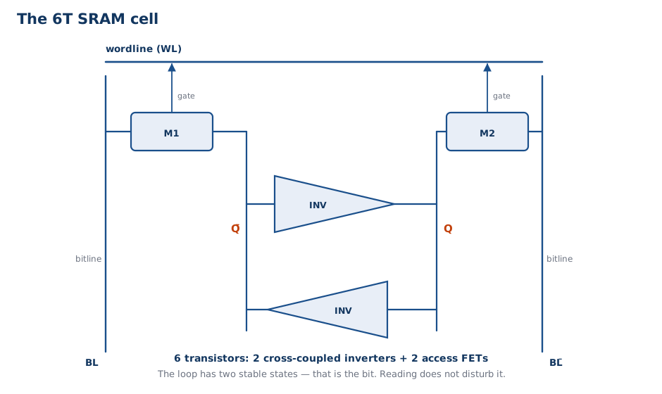
Six transistors, and the bit is held by feedback — no refresh, no capacitor, and reading it does not destroy it.
SRAM: Reading and Writing
Read — precharge both bitlines high and let them float, raise the wordline, and let the cell pull one bitline down. A sense amplifier resolves the small difference.
- The cell only pulls down; it never drives high. So the read is non-destructive.
Write — drive the bitlines hard to the desired values, raise the wordline, and overpower the cell’s feedback loop so it flips.
The access transistors must be sized so that a bitline at 0 can overpower a cell holding 1 — but a bitline at 1 must not overpower a cell holding 0.
Why the asymmetry? (Think about it before the next slide.)
Why SRAM Cannot Be Large
Two limits, both physical:
- Six transistors per bit. A 64 KB cache is half a million transistors before you count the tags, the decoders, or the sense amps.
- Wires dominate. An N-entry multiported SRAM needs N wordlines and 2N bitlines crossing the array. The wire area grows as O(N²).
This is why “just make the L1 bigger” is not free, and why register files are tiny and multiported while caches are large and single-ported.
DRAM: the 1T Cell
One transistor and one capacitor. The charge on the capacitor is the bit.
Consequences, all of them annoying:
- The capacitor leaks — every cell must be refreshed every few milliseconds.
- Reading shares charge between the capacitor and the bitline — so the read is destructive, and the value must be written back.
- The voltage swing is tiny, so every bitline needs a sense amplifier.
~20× denser than SRAM, and 2–10× slower. That is the trade, and it is a good one for main memory.
Flash and Disk
Flash — a floating gate traps electrons. Trapped charge means the transistor never inverts, so the cell reads as permanently off. No power needed to hold the bit.
- Very dense, non-volatile, no refresh
- Slow to write (10–100 µs), and writing damages the oxide: ~10³–10⁵ cycles
Disk — a magnetic domain, read by a head on a moving arm.
- ~10 ms to move the head: five orders of magnitude worse than DRAM
- But ~100× cheaper per bit, and it does not wear out
Flash and disk are why the hierarchy continues below DRAM — and why “swap” exists.
Size Is a Fundamental Limit
“Size is a fundamental limit, even setting cost aside.”
Why: a bigger array means longer bitlines, which means more capacitance, which means a smaller voltage swing, which takes longer to sense.
Latency grows with capacity by physics, not by bad engineering. You cannot buy your way out of it with a bigger budget or a better process node.
So a large, fast memory is impossible. If we want the behaviour of one, we have to fake it — and that is what the rest of this lecture is about.
…Unless You Stack It
The 2026 answer to “size is a fundamental limit” was not to scale the array. It was to put a second die on top of it.
AMD’s 3D V-Cache: a separate silicon die containing 64 MB of SRAM, bonded directly underneath the compute die and wired into the L3.
- Ryzen 7 9850X3D: 32 MB of on-die L3 + 64 MB stacked = 96 MB
- Same physics, different trick — the hierarchy got deeper by packaging
MIT’s 2017 deck says size is a fundamental limit. The industry’s response was to stop fighting it and start stacking.
Part II — Locality
The Locality Principle
Access to address X at time t implies access to X + ΔX at time t + Δt becomes more probable as ΔX and Δt approach zero.
Two special cases, and both matter:
- Temporal locality — ΔX = 0. You will touch the same address again soon.
- Spatial locality — Δt = 0. You will touch a nearby address soon.
This is an empirical claim about real programs, not a theorem. Compilers and programmers create it — and sometimes destroy it.
Reference Patterns and the Working Set
Plot address against time and real programs do not fill the space. They draw structured patterns, and each one is a different kind of locality:
- code (bottom) — ascending ramps: straight-line execution walking forward, then a branch back to the top of the loop. Each ramp is spatial locality; the ramps repeating at the same addresses is temporal locality.
- stack (middle) — drifts slowly upward in small clusters: frames pushed on a call, popped on return.
- data (top) — a handful of blobs that move around: a few live structures, not the whole array.
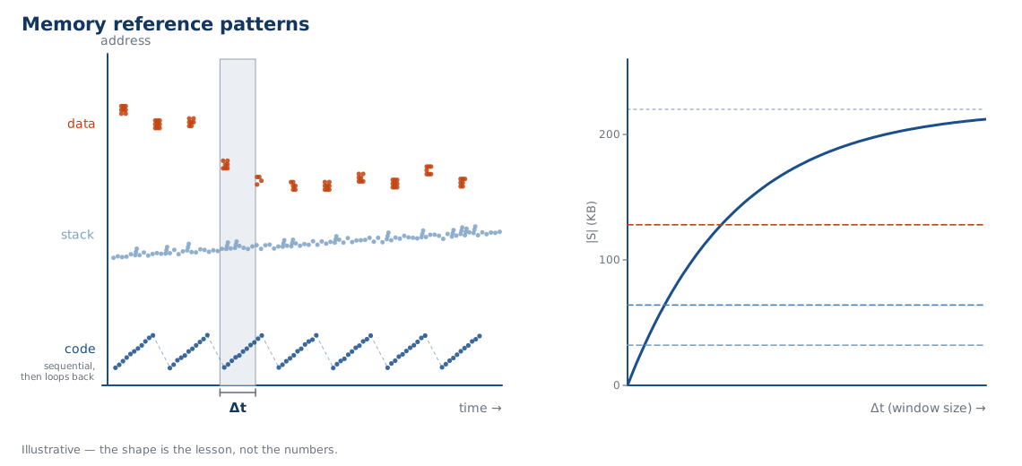
Pick a window Δt and count the distinct addresses touched. That set is the working set |S|. It grows with Δt, then saturates at the program’s real footprint.
That saturation is the whole opportunity: a cache bigger than the saturated working set sees mostly hits.
Everything Is a Cache for Something Else
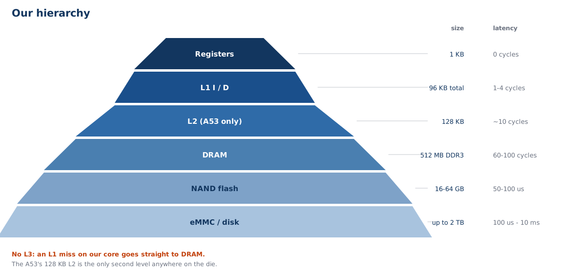
Each level is a cache for the level below it — and each has a different owner: the compiler allocates registers, hardware manages the caches, the OS runs the flash page cache. Same problem, three different owners.
Expose or Hide?
Two ways to give a programmer a hierarchy:
Expose it. “Here are two memories. Put the hot data in the fast one yourself.” Scratchpad memory, DSPs, some GPUs, and — partly — our ION carveouts.
Hide it. One flat address space. Hardware (and the OS) decide where data lives. That is a cache.
Every real system does both. Ours does both: the caches hide, and the carveouts expose.
Part III — AMAT: The One Equation
Hit, Miss, and Two Ratios
A cache is asked for an address. There are exactly two outcomes:
| Outcome | What happens | Cost |
|---|---|---|
| Hit | the block is present; return it | hit time (a few cycles) |
| Miss | not present; fetch the block, evict something, return it | hit time + miss penalty |
- Hit ratio (HR) = hits / total accesses
- Miss ratio (MR) = 1 − HR
The processor now has variable memory access time, and something has to cope with that — either stall the pipeline, or keep going out of order.
AMAT
The average memory access time:
\[\text{AMAT} = \text{HitTime} + \text{MissRatio} \times \text{MissPenalty}\]
Read it as: every access pays the hit time, and a fraction of them pay the penalty on top.
Two reasons this is the right metric:
- It is per access, so it multiplies cleanly by the instruction count.
- It composes — the miss penalty of one level is the AMAT of the next.
AMAT Composes
The miss penalty of level 1 is the AMAT of level 2:
\[\text{AMAT} = \text{HT}_1 + \text{MR}_1 \times \bigl(\text{HT}_2 + \text{MR}_2 \times \text{Penalty}_{\text{mem}}\bigr)\]
Now apply it to our two big cores, with the same L1 hit ratio of 0.95:
| Core | Hierarchy | AMAT |
|---|---|---|
| C906 | L1 → DDR3 | 2 + 0.05 × 80 = 6.0 cycles |
| A53 | L1 → L2 → DDR3 | 2 + 0.05 × (10 + 0.20 × 80) = 3.3 cycles |
Same L1. Same hit ratio. The L2 nearly halves the AMAT — because it catches most of the 5% that miss L1.
What Hit Ratio Do You Need?
Suppose a hit costs 2 cycles and a miss costs 100.
| Target | Equation | Required HR |
|---|---|---|
| Beat no cache at all (AMAT < 100) | 100 = 2 + (1−HR)·100 |
2% |
| AMAT = 10 cycles | 10 = 2 + (1−HR)·100 |
92% |
| AMAT = 5 cycles | 5 = 2 + (1−HR)·100 |
97% |
Even a terrible cache beats no cache. But a good one has to be very good indeed — the last few percent of hit ratio is where all the engineering lives.
The Honest Caveat
That “80 cycles” is an estimate, not a measurement. It is DDR3 CAS latency plus tRCD plus controller scheduling, and the controller is allowed to reorder.
- Bandwidth floor: one 64-byte line at peak 1866 Mbps × 16 bit = 3.73 GB/s is
64 B ÷ 3.73 GB/s≈ 17 ns ≈ 17 cycles at 1 GHz. - Latency is several times that, because a single random read cannot use peak bandwidth.
We do not need the exact number to reason about caches. We need the shape: hit time is single digits, miss penalty is double digits.
Part IV — How a Cache Works
The Basic Algorithm
The pseudocode hides the two questions that define a cache:
- How do we search? → direct-mapped, set-associative, fully-associative
- Which line do we evict? → the replacement policy
Direct-Mapped: the Simplest Search
One place for each block. Block number modulo the number of lines.
Each line stores a valid bit, a tag, and the data:
| index | valid | tag | data |
|---|---|---|---|
| 0 | 1 | 0x20000 |
64 bytes |
| 1 | 0 | — | — |
| 2 | 1 | 0x1F4A3 |
64 bytes |
| … | |||
| 255 | 1 | 0x20001 |
64 bytes |
Search: index the array, compare one tag. That is a single comparator, not a search.
A Worked Lookup on Our D-Cache
Our L1 D-cache: 64 KB, 4-way, 64 B lines ⇒ 256 sets. A 32-bit address splits as tag 18 | index 8 | offset 6.
| Address | offset | index | tag | Result |
|---|---|---|---|---|
0x8000_1040 |
0x00 |
0x41 (65) |
0x20000 |
load it into set 65 |
0x8000_1040 again |
0x00 |
0x41 |
0x20000 |
HIT |
0x8000_5040 |
0x00 |
0x41 |
0x20001 |
different tag — MISS |
Both addresses land in set 65. In a direct-mapped cache they would evict each other forever. In ours, both can live there — we have four ways.
Part of the Address Is Encoded in the Location
The index bits are not stored anywhere. They are implied by which line you looked in — the hardware computed them from the address.
So the tag array only needs the top bits:
| Cache | Sets × ways | Metadata per line | Tag array total |
|---|---|---|---|
| Direct-mapped 64 KB | 1024 × 1 | 18 tag + 1 valid + 1 dirty | 640 B |
| Our 4-way 64 KB | 256 × 4 | 18 tag + 1 valid + 1 dirty | 2.5 KB |
The address is partly stored in the location. That is what makes a cheap, one-comparator search possible — and it is also the source of conflict misses.
Block Size: the Third Field
The address now has three fields, not two:
The block offset selects a byte inside the line. It costs nothing to store — it is pure address arithmetic — and it buys you spatial locality for free.
So why not make blocks enormous? Because a bigger block means:
- fewer blocks for the same capacity → more conflicts
- a longer fill: you must fetch the whole line before you can use any of it
- wasted bandwidth if you never touch the rest of the line
Block Size Tradeoffs
AMAT is U-shaped in block size, because two effects fight: bigger blocks cut the miss rate (more spatial reuse per fetch) but raise the miss penalty (a longer fill before you can use any of it).
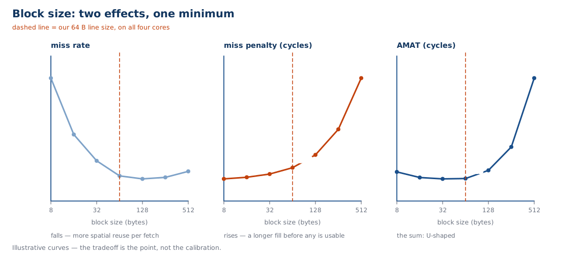
MIT’s deck puts the optimum at about 64 bytes (slide 28). Our C906’s line size is exactly 64 bytes, on both caches.
That is not a coincidence. It is the same optimum, found independently.
Conflict Misses
Misses come in three kinds:
- Compulsory (cold) — first touch. Unavoidable.
- Capacity — the working set is bigger than the cache. Unavoidable at that size.
- Conflict — the working set fits, but maps to too few sets. Avoidable.
A concrete case on our D-cache. A row of this matrix is exactly 16 KB:
Every A[i][0] is 16 KB after the last — 256 lines apart — so they all land in the same set. Four fit in four ways. The fifth thrashes, forever.
Fully Associative
No index at all. A block may live in any line.
To search, compare the tag against every line in parallel — that is a CAM, and it costs one comparator and one tag read per line.
| Direct-mapped | Fully associative | |
|---|---|---|
| Search cost | 1 comparator | N comparators |
| Conflict misses | many | none |
| Data select | none | N:1 mux |
Used where N is small and misses are expensive: our μTLBs are 10-entry fully associative, and the branch target buffer is 16-entry fully associative.
N-Way Set Associative
The compromise. Draw the cache as a grid:
A block maps to one row (chosen by the index) and may occupy any column.
Direct-mapped is 1-way. Fully associative is 1 set.
It is exactly N direct-mapped caches in parallel, sharing an index.
N-Way Structure
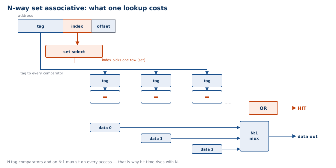
Cost: N comparators and an N:1 mux on the critical path. Hit time grows with N.
That is the tension: more ways means fewer conflict misses, but every access pays for the extra comparators.
Associativity Tradeoffs
AMAT versus associativity is also U-shaped: conflict misses fall, hit time rises.
“Little additional benefit beyond 4 to 8 ways.” — H&P, cited on MIT slide 34
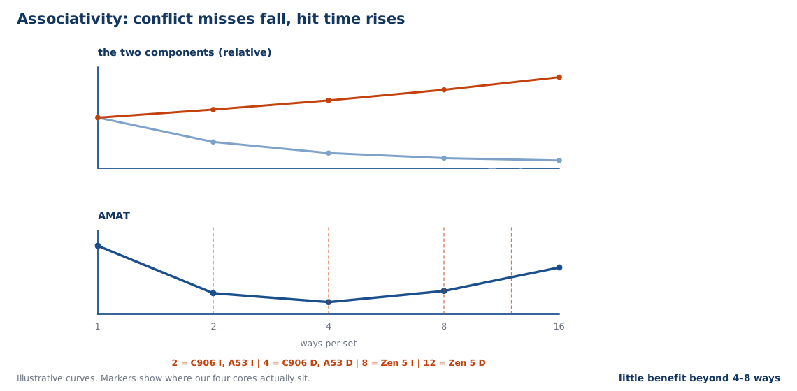
All four of our cores sit on that curve. Zen 5 raised its L1 D-cache from 8-way to 12-way specifically to accommodate the larger 48 KB size — the tradeoff, visible in a shipping product.
Replacement Policy
Only matters when ways > 1 — you must choose a victim.
| Policy | Rule | Cost |
|---|---|---|
| Belady’s MIN | evict the block used furthest in the future | optimal; needs the future — unimplementable |
| LRU | evict the least recently used | good; needs ~log₂(N!) bits per set |
| FIFO | evict the longest-resident | cheap; log₂(N) bits — but not a stack algorithm |
| Random | evict at random | no state; no adversarial pattern |
Belady’s MIN is still useful: it is the lower bound you measure other policies against.
And no core on our board implements true LRU — the C906 uses FIFO, the A53 uses pseudo-random, x86 uses an approximation. The textbook policy is the reference, not the implementation.
Why FIFO Is Different
FIFO is not a stack algorithm — it does not obey the inclusion property. The consequence is Belady’s anomaly: giving it more capacity can make it worse.
Classic reference string, three frames versus four:
| Frames | Faults |
|---|---|
| 3 | 9 |
| 4 | 10 |
More cache, more misses. LRU cannot do this — it is a stack algorithm, so a bigger cache always contains the smaller one’s contents.
In practice FIFO is usually fine. But “usually fine” is a different claim from “cannot be worse”, and our D-cache makes the weaker one.
Write Policy
Reads are easy. Writes force a choice — and a second one on a write miss:
| Policy | On a write | Cost |
|---|---|---|
| Write-through | write cache and memory | simple, no dirty bit — but every store costs bandwidth |
| Write-behind | write a buffer, drain later | core does not stall; still full bandwidth |
| Write-back | write only the cache; memory on eviction | fastest, lowest bandwidth — needs a dirty bit |
And on a write miss: write-allocate (fetch the block first) or write-no-allocate (write straight through)?
Our C906 D-cache: write-back, with write-allocate / write-no-allocate configurable — and an adaptive mode we will meet in Part V.
Dirty Bits
One extra bit per line. It answers: does memory match this line?
- WRITE to a line → set
dirty = 1 - Evict a line → write it back only if
dirty == 1 - Fill a line from memory →
dirty = 0
The consequence is uncomfortable: main memory can be stale. DRAM is not the truth; the cache is. Everything that bypasses the cache — DMA, another core, a debugger — now has a coherency problem.
Part V — Four Cores, Four Answers
Four Cores, Four Answers
Everything so far was the model. Here is what four real cores did with it.
| C906 @ 1 GHz | C906 @ 700 MHz | Cortex-A53 | Ryzen 7 9850X3D | |
|---|---|---|---|---|
| L1 I | 32 KB, 2-way | 16 KB, 2-way | 32 KB, 2-way | 32 KB, 8-way |
| L1 D | 64 KB, 4-way | 16 KB, 4-way | 32 KB, 4-way | 48 KB, 12-way |
| L2 | — | — | 128 KB, 16-way | 1 MB, 16-way |
| L3 | — | — | — | 96 MB |
| Line | 64 B | 64 B | 64 B | 64 B |
| Replacement | FIFO | FIFO | pseudo-random | n/d |
| Prefetch | yes, both | yes, both | n/d | yes |
Associativity runs 2 → 4 → 8 → 12. L3 runs none → none → none → 96 MB.
But look at the first two columns of associativity: the C906 and the A53 are identical — 2-way instruction, 4-way data. And the line size is 64 bytes on all four. Two of those columns are industry consensus.
Two C906s, Not One
The SG2000 has two C906 cores, and they are not the same core:
| Big C906 | Little C906 | |
|---|---|---|
| Clock | 1.0 GHz | 700 MHz |
| L1 I | 32 KB | 16 KB |
| L1 D | 64 KB | 16 KB |
| Runs | Linux | FreeRTOS / bare metal |
| MMU | yes | M-mode, physical |
Half the clock — but half the I-cache and a quarter of the D-cache. A memory-bound workload on the little core loses far more than 30%: it loses on capacity and on latency at the same time.
C906 L1 I-Cache: 2-Way
Straight from the manual (§7.1):
| Property | Value |
|---|---|
| Size | 8 / 16 / 32 / 64 KB, hardware-configurable |
| Associativity | 2-way set associative |
| Line | 64 B |
| Indexing | VIPT — virtual index, physical tag |
| Read width | 32 bits |
| Refill width | 128 bits |
| Replacement | FIFO |
| Maintenance | whole-cache and single-line invalidate |
| Prefetch | yes — MHINT.IPLD, same page only |
2-way is the bottom of the useful range — the minimum that removes the worst conflict misses without paying for comparators on the fetch path.
C906 L1 D-Cache: 4-Way
§7.2 — and note how much more there is to say than for the I-cache:
| Property | Value |
|---|---|
| Size | 8 / 16 / 32 / 64 KB, hardware-configurable |
| Associativity | 4-way set associative |
| Line | 64 B |
| Indexing | VIPT |
| Read / write width | 64 bits / 128 bits |
| Write policy | write-back, write-allocate or write-no-allocate (configurable) |
| Replacement | FIFO |
| Prefetch | sequential and strided (stride ≤ 16 lines, forward and backward) |
| Extra | adaptive write-allocate; LR/SC local monitor |
The D-cache is where the interesting engineering is. Every row past “line size” is an optimization the I-cache does not need.
Two Vendors, One Answer
The C906 splits its Harvard cache: I-cache 2-way, D-cache 4-way.
The Cortex-A53 — different vendor, different ISA, same die — splits it exactly the same way:
| L1 I | L1 D | |
|---|---|---|
| C906 @ 1 GHz | 32 KB, 2-way | 64 KB, 4-way |
| Cortex-A53 | 32 KB, 2-way | 32 KB, 4-way |
Neither manual explains the choice. But two independent design teams landing on 2/4 is not a coincidence — it is a consensus, and consensus usually has a reason.
Two hypotheses, and they are not mutually exclusive:
- The I-cache sits on the fetch critical path — every comparator added there delays every instruction fetch, so it is kept minimal.
- Instruction streams are regular and sequential with few conflicts, so the extra ways buy less on the I side than on the D side.
The A53 Has an L2. We Don’t.
| C906 @ 1 GHz | Cortex-A53 @ 1 GHz | |
|---|---|---|
| L1 I | 32 KB, 2-way | 32 KB, 2-way |
| L1 D | 64 KB, 4-way | 32 KB, 4-way |
| L2 | none | 128 KB, 16-way |
| On an L1 miss | straight to DDR3 | L2 first |
Back to the AMAT composition, same 0.95 L1 hit ratio:
| AMAT | |
|---|---|
C906: 2 + 0.05 × 80 |
6.0 cycles |
A53: 2 + 0.05 × (10 + 0.20 × 80) |
3.3 cycles |
Identical associativity. Identical line size. The C906 even has twice the L1 D-cache — and it still loses, because there is nothing behind it to absorb a miss.
Our Bit Arithmetic
Apply the three-field split to all four of our caches. Line size is 64 B everywhere, so the offset is always 6 bits:
| Core | Cache | Size | Ways | Sets | index | offset | tag |
|---|---|---|---|---|---|---|---|
| C906 1 GHz | I | 32 KB | 2 | 256 | 8 | 6 | 18 |
| C906 1 GHz | D | 64 KB | 4 | 256 | 8 | 6 | 18 |
| C906 700 MHz | I | 16 KB | 2 | 128 | 7 | 6 | 19 |
| C906 700 MHz | D | 16 KB | 4 | 64 | 6 | 6 | 20 |
Both 1 GHz caches land on 256 sets and 8 index bits — different sizes, same geometry. The 64 KB D-cache gets its extra capacity from the fourth way, not from more sets.
VIPT: Why the Index Can Be Virtual
VIPT = virtual index, physical tag. Why bother?
The index needs no translation, so the TLB lookup and the set selection run at the same time. With a physical index you would have to translate first, then index — two serial latencies on every access.
The constraint: the index bits must lie entirely inside the page offset. Otherwise two virtual addresses for the same physical page could pick different sets — synonyms.
\[\text{sets} \times \text{line size} \le \text{page size}\]
The Open Question
Our 1 GHz caches: 256 sets × 64 B = 16 KB. Our small page size: 4 KB.
\[16\ \text{KB} > 4\ \text{KB}\]
So two of the eight index bits come from the virtual page number, not from the page offset. Which means the hardware is either:
- using “VIPT” loosely, and cacheable mappings must use ≥ 16 KB pages;
- doing something undocumented to handle synonyms; or
- accepting aliasing, and relying on the OS never to create it.
The manual does not say. We do not know. This is a real, checkable open question about the chip in your hand — and a good one.
Write-Back, Prefetch, and Adaptive Allocation
Three mechanisms on our D-cache that MIT’s taxonomy does not contain:
- Write-back with a dirty bit — exactly as taught, no surprise.
- Strided prefetch — the LSU detects a miss pattern and prefetches up to 16 lines ahead, forward or backward. It manufactures spatial locality that is not there.
- Adaptive write-allocate — after N consecutive line writes (
HINT.AMRL1), the page’s write-allocate property switches off automatically.
That last one is the memset problem, solved in hardware: if you are writing a whole buffer, fetching each line before overwriting it is pure waste. The cache notices and stops doing it.
Part VI — Synthesis
What We Actually Learned
- The hierarchy is forced. A large fast memory cannot be built — latency grows with array size by physics. Stacking dies is the only recent escape.
- Locality is the load-bearing assumption. If programs accessed memory uniformly, every technique here would be worthless.
- AMAT is the whole game.
HitTime + MissRatio × MissPenalty. Every mechanism in the lecture moves one of those three terms. - Associativity, block size, and replacement are three answers to two questions. How do we search, and whom do we evict.
- Our four cores are all on the same curves — 2, 4, 8, 12 ways; 64-byte lines; none to 96 MB of L3.
The textbook model is not wrong. It is under-specified — and the places where real silicon fills in the gaps are exactly where the engineering lives.
Discussion Prompts
- Both the C906 and the A53 are 2-way on instructions and 4-way on data. Argue for or against keeping the two sides symmetric — and say what evidence would settle it.
- The A53 has 32 KB + 32 KB + 128 KB; the C906 has 32 KB + 64 KB and no L2. Which would you rather compile for, and does the answer depend on the program?
- Adaptive write-allocate turns itself off under streaming stores. What could go wrong with a mechanism that changes policy based on observed history?
- The VIPT constraint appears to be violated at 4 KB pages. Design an experiment that would settle it.
- Given
AMAT = HT + MR × MP, and a fixed transistor budget, where do you spend it — more ways, more sets, or an L2?
Every one of these is answerable from the material in this deck. None has a single right answer.
Refs
Primary sources for this deck
- XuanTie C906 User Manual (openc906), §7 memory subsystem, §5 MMU, §7.3 cache operations — the L1 geometry, FIFO policy, and prefetch mechanisms.
- SG2000 / SG2002 Technical Reference Manuals — the core configurations and the address map.
- MIT 6.004 Computation Structures, Spring 2017, lecture 14 — the structure of the stock story, and the AMAT framing.
- Hennessy & Patterson, Computer Architecture, cache chapter — associativity tradeoffs, replacement policies.
- AMD Zen 5 microarchitecture tables and the Ryzen 7 9850X3D product page — the x86 comparison.
CS 4250 · Caches and the Memory Hierarchy — SG2000